


.png)
While the Kria KR260 can be used straight out of the box with no previous FPGA design experience, I think it's import to provide the resources for those interested in getting into FPGA design using their Kria KR260.
There are three main development tools in the Xilinx ecosystem: Vivado, Vitis, and PetaLinux. Vivado is the IDE for developing the hardware in Verilog or VHDL for the programmable logic design of a Xilinx FPGA. Vitis is a software development IDE for writing bare metal or Linux C/C++ applications that run on either a physical ARM-core processor or soft-core processor in the Xilinx FPGA. And PetaLinux is a set of software tools based on the open-source Yocto project for developing an embedded Linux image for Xilinx FPGAs.
Since both Vitis and PetaLinux need a base hardware design for the software to run on, Vivado is the starting point for any custom FPGA design on a Xilinx chip. So this project walks through the entire process of creating a custom hardware design in Vivado for the Kria KR260 development SoM board including the hooks for hardware acceleration and making note of where a user can add to the design.
Create Vivado Project
Source the Vivado toolset and launch the GUI:
~$ source /tools/Xilinx/Vivado/2022.1/settings64.sh ~$ vivado
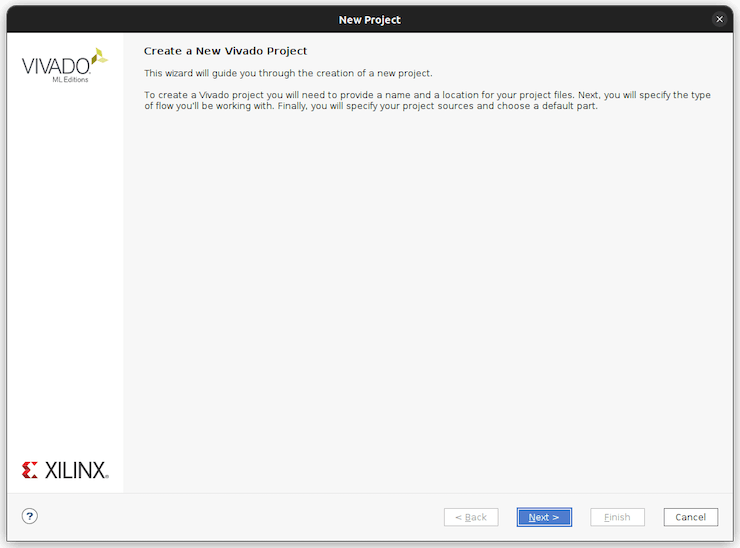
Select the option under Quick Start for Create Project:

Walking through the project setup pages, give the project the desired name and select the desired directory for it. Be sure to check the option on the Project Type window that the Project is an extensible Vitis platform, this is the first hook required for a hardware accelerated design.
Vivado comes with board preset files you can select to set the base configuration in a project that are necessary for any FPGA development board (such as DDR pin-out and configuration) and needs to be setup for every project regardless of a user's custom design. In the Default Part page, switch to the Boards tab and click Refresh, then search for kr260. Single click on the row for the Kria KR260 Robotics Starter Kit and click Next.
The final page is just a summary of the selections just made for the project that's about to be created. Click Finish to create the new Vivado project.
1 / 5
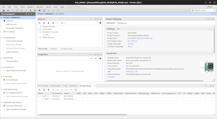
Once the project is generated, it opens to a blank project manager page.
Create Block Design
First things first in a new Vivado design is to create a block design. A block design is a graphical block programming tool where each block represents a chunk of HDL code that is configured and connected together via this GUI. It's the easiest way for a user not already familiar with any HDL language to get started in FPGA design.
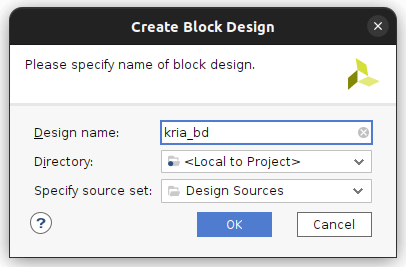
In the Project Manager window under the IP Integrator tab, select the Create Block Design option and give it the desired name in the following pop up window.
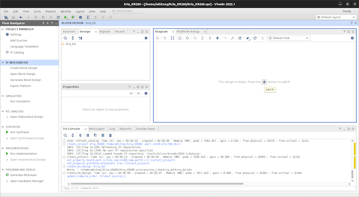
After a few moments, a black block design will open:

The first thing that needs to be defined in a block design is the processor. In the case of the Kria, it has a physical ARM-core processor built into the fabric of the programmable logic. To instantiate it in the block design to be able to configure it and connect other IP blocks to it, click the + button in the Diagram window and search for "zynq".
Double-click the Zynq MPSoC IP to add it to the block design. This IP block is how the ARM-core processor's hardware settings can be customized by a user in the Kria SoM. A green banner will appear at the top of the Diagram window with the option to Run Block Automation. Block automation will apply the specific KR260 board presets to the Zynq MPSoC IP block.
1 / 2
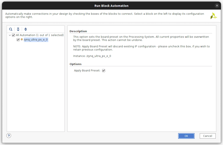
Click the link for Run Block Automation and ensure that the option to Apply Board Preset is checked in the window that pops up before clicking OK.
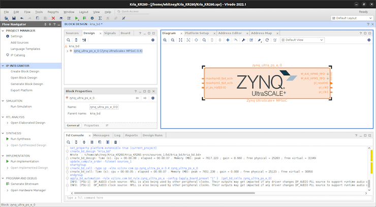
The ports on the Zynq UltraScale+ IP block will change slightly with the application of the KR260 board presets:
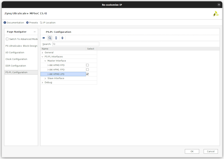
Since I'm adding hooks for hardware acceleration (which means configuring the hardware here in Vivado so that I'll have access to it from the software in Vitis/PetaLinux later) there are a few customizations to the Zynq UltraScale+ IP.
To customize an IP in the block design, simply double-click on it to bring up the configuration window.
What I'm doing is simply disabling the two full-power high performance AXI ports in the block design and enabling the low-power high performance AXI port:
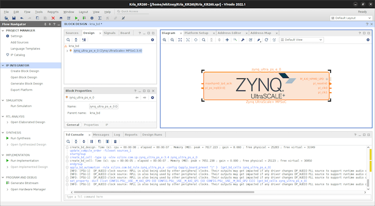
This is simply to make sure that I don't ever accidentally use the two full-power high performance AXI ports in future updates of this hardware design in the block design because I want them saved solely for hardware acceleration later on (which is addressed later on in the Platform Setup step).
This is something that's a little counter-intuitive about hardware acceleration in Vivado is that disabling something in the block design doesn't disable it completely in the whole project, it's still an option to enable in the Platform Setup step to make available to the software in Vitis.
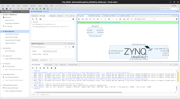
Next I'm adding a clocking wizard IP to my design as a clock source controlled by the Zynq UltraScale+ IP that I can enable in the Platform Setup step to make available to the software in Vitis for hardware acceleration.
1 / 2
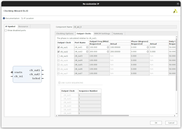
Double-click the clocking wizard IP to customize it. In the Output Clocks tab, enable the desired number of output clocks with desired rates and change the polarity of the reset to match that of the reset coming from the Zynq UltraScale+ IP block (which is active low).
1 / 2
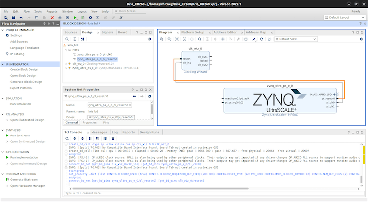
Connect the pl_clk0 output of the Zynq UltraScale+ IP to the clk_in1 pin of the clocking wizard IP and the pl_reset0 output of the Zynq UltraScale+ IP to the resetn pin of the clocking wizard IP.
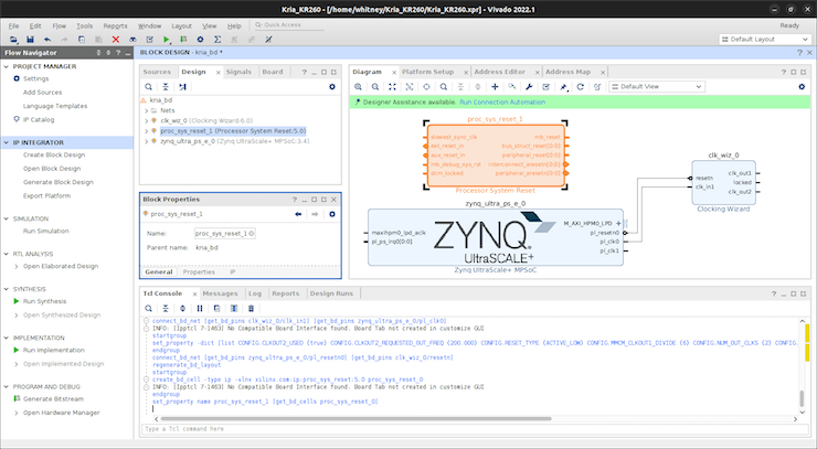
Add Processor System Reset IP blocks for each of the output clocks of the clocking wizard IP and connect the ext_reset_in of each to the pl_reset0 output of the Zynq UltraScale+ IP. Connect clk_outn of the clocking wizard IP to the slowest_sync_clk of each respective Processor System Reset IP.
All of the connection automation options can be ignored and they will disappear once the connections described above are made.
1 / 4
Some sort of interrupt source is also needed for hardware accelerated designs. To meet this requirement, add an AXI interrupt controller IP. AXI is a standard interface that Xilinx uses in their designs as a connection interface for IP blocks in a hardware design because it's highly configurable and the connection process can be automated.
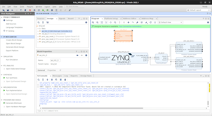
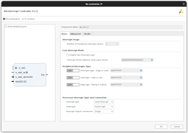
After adding the AXI interrupt controller IP, double-click on the block and change the Interrupt Output Connection from Bus to Single.
Then select the option to Run Connection Automation which will automatically configure and connect the AXI interrupt controller to the Zynq UltraScale+ IP via the AXI interface.
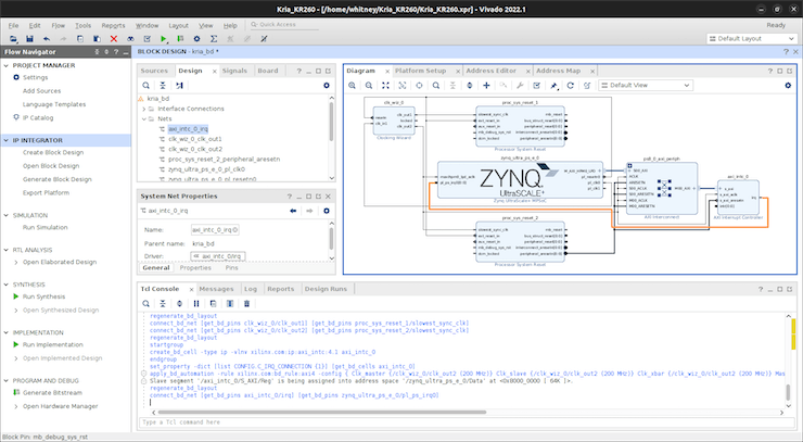
In the configuration window for the connection automation, select the clock for the AXI interface that you plan to make the default for the hardware acceleration design. In my case, that is the 200 MHz clk_out2 from the clocking wizard IP. Whichever clock you chose, be sure that the clock source for the driving bridge IP, slave interface, and master interface are all set to the same clock source.

Finally, connect the irq output from the AXI interrupt controller IP to the pl_ps_irq input of the Zynq UltraScale+ IP.
%20(2).png)
%20(1).png)
%20(22).png)
%20(20).png)
%20(19).png)
%20(18).png)
%20(2).png)
%20(4).png)
%20(5).png)
%20(10).png)
.png)
%20(1).png)
%20(10).png)
%20(8).png)
%20(7).png)
%20(2).png)
.png)
%20(1).jpg)
%20(6).png)
%20(5).png)
%20(4).png)
%20(3).png)
%20(1).png)
.png)


.png)

%20(1).png)
.png)
.png)
%20(2).png)
.png)

.png)


